Xiangdafeng Technology (Beijing) Co., Ltd Copyright No.2020041289-1
Address:712, 7th floor, building 154, brick factory Beili, Tongzhou District, Beijing
Mobile:+86 18901353186 Tel:010-82900580
Fax:010-82900580Mail:market@xdfpcba.com
SMT basic process elements include: screen printing (or dispensing), mounting (curing), reflow soldering, cleaning, testing, repair

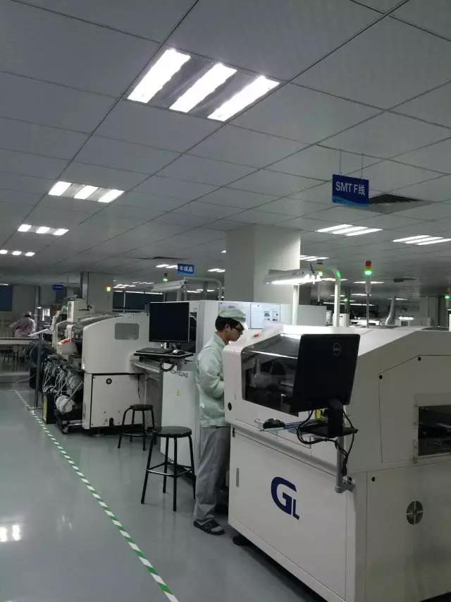
Printing: its role is to solder paste or paste to the PCB pad, to prepare for the welding of components. The equipment used is screen printing machine (solder paste printing machine), which is located at the front end of SMT production line.
Dispensing: it drops glue to the fixed position of PCB, and its main function is to fix components to PCB. The equipment used is dispensing machine, which is located at the front end of SMT production line or behind the detection equipment.
Mounting: its function is to accurately mount the surface mount components to the fixed position of PCB. The equipment used is SMT machine, which is located behind the screen printing machine in SMT production line.
Curing: its function is to melt the adhesive, so that the surface assembly components and PCB board are firmly bonded together. The equipment used is curing furnace, which is located behind the placement machine in SMT production line.
Reflow soldering: its function is to melt the solder paste, so that the surface assembly components and PCB board are firmly bonded together. The equipment used is reflow soldering furnace, which is located in the back of SMT production line.
Cleaning: its function is to remove the harmful welding residues such as flux on the assembled PCB board. The equipment used for cleaning machine, position can not be fixed, can be online, can not be online.
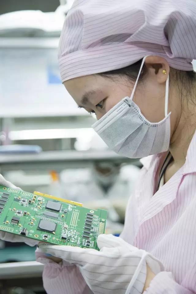
Detection: its function is to detect the welding quality and assembly quality of the assembled PCB. The equipment used includes magnifying glass, microscope, on-line tester (ICT), flying needle tester, automatic optical inspection (AOI), X-ray detection system, function tester, etc. According to the needs of detection, the position can be configured in the right place of the production line.
Repair: its role is to detect the PCB board failure rework. The tools used are soldering iron, repair workstation, etc. Configuration in any position in the production line.
1、 Single side assembly
Incoming inspection = > screen printing solder paste (spot mounting adhesive) = > mounting = > drying (curing) = > reflow soldering = >
Cleaning = > detection = > repair
2、 Double sided assembly
A: Incoming material detection = > A-side screen printing solder paste of PCB (spot mounting adhesive) = > mounting = > drying (curing) = >
Reflow soldering on a side = > cleaning = > flipping = > silk screen solder paste on B side of PCB (spot mounting adhesive) = > patch = >
Drying = > reflow soldering (preferably only for B side = > cleaning = > detection = > repair)
This process is suitable for PCB with large SMD such as PLCC on both sides.
B: Incoming material detection = > A-side screen printing solder paste of PCB (spot mounting adhesive) = > mounting = > drying (curing) = >
Reflow soldering on a side = > cleaning = > flipping = > patch adhesive on B side of PCB = > patch = > curing = >
B-side wave soldering = > cleaning = > inspection = > repair)
This process is suitable for reflow soldering on a side and wave soldering on B side of PCB. This process should be used when only sot or SOIC (28) pins are below in the SMD assembled on the B side of PCB.

3、 Single side mixed loading process
Incoming material inspection = > PCB A-side silk printing solder paste (spot adhesive) = > patch = > drying (curing) = > reflow welding = > cleaning = > plug-in = > wave soldering = > cleaning = > inspection = > repair
4、 Double side mixed loading process
A: Incoming material inspection = > PCB B-point patch = > patch = > curing = > flip over = > PCB A-side plug-in = > wave soldering = > cleaning = > detection = > repair
Paste first and then insert ➡ For SMD components more than separated components
B: Incoming material inspection = > PCB A-side plug-in (pin bending) = > flip over = > PCB B-point patch adhesive = > patch = > curing = > flip over = > wave soldering = > cleaning = > detection = > repair
Insert and paste first → applicable to the case where the separation element is more than SMD element
C: Incoming material inspection = > PCB A-side silk printing solder paste = > patch = > drying = > reflow welding = > plug-in, pin bending = > flip over = > PCB b-spot patch = > patch = > curing = > flip over = > wave soldering = > cleaning = > detection = > repair
Mixed loading on a side and mounting on side B
D: Incoming material inspection = > PCB b-spot adhesive = > patch = > curing = > flip over = >pcb A-side silk paste = > patch = > A-side reflow welding = > plug-in = > wave soldering on side B = > cleaning = > detection = > repair

A side mixed, B side mounted
SMD on both sides, reflow soldering, plug-in, wave soldering
E: Incoming inspection = > B-side screen printing solder paste of PCB (spot solder) = > patch = > drying (curing) = > reflow soldering = > flap = > A-side screen printing solder paste of PCB = > patch = > drying = > reflow soldering 1 (local soldering can be used) = > plug-in = > Wave soldering 2 (manual soldering can be used if there are few plug-in components) = > cleaning = > detection = > repair
5、 Double sided assembly process
A: Incoming material detection, A-side screen printing solder paste (spot mounting adhesive), mounting, drying (curing), A-side reflow soldering, cleaning, turnover of PCB; B-side screen printing solder paste (spot mounting adhesive), mounting, drying, reflow soldering of PCB (preferably only for B-side, cleaning, testing, repair)
This process is suitable for PCB with large SMD such as PLCC on both sides.
B: Incoming material detection, A-side screen printing solder paste (spot paste), patch, drying (curing), A-side reflow soldering
Consultation hotline
010-82900580