


Xiangdafeng Technology (Beijing) Co., Ltd Copyright No.2020041289-1
Address:712, 7th floor, building 154, brick factory Beili, Tongzhou District, Beijing
Mobile:+86 18901353186 Tel:010-82900580
Fax:010-82900580Mail:market@xdfpcba.com


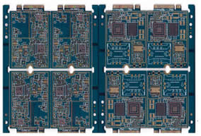
We have professional PCB designers, with more than 5 years of industry experience per capita and more than 8 years of senior employees. Can independently complete PC motherboard, industrial control board, notebook motherboard, medical devices, mobile phones, digital cameras, communication electronics and other products of high-speed, high-density, digital analog hybrid layout design. Our engineers have an extremely detailed and thorough understanding of multi-layer PCB boards, and have a better understanding of the structure and wiring specifications of high-end PCB boards with blind buried holes.

| Circuit board design of communication products | GSM/GPRS、Switch、RF Equipment, etc |
| Circuit board design of digital / Digital products | Set top box, HDTV, digital camera, video camera, etc |
| Circuit board design of security products | Video monitoring, intercom, etc |
| Circuit board design of PC and related products | MB, Nb, server motherboards and various industrial control boards |
Schematic diagram:A complete electronic document format with correct netlist can be generated;
Mechanical dimension:Provide specific location, direction identification of positioning device, and identification of specific height limit location area;
BOM Detailed list:The main purpose is to determine and check the package information of the device on the schematic diagram;
Wiring Guide:The description of specific requirements for special signals, as well as the design requirements of impedance and lamination.
Allegro,PADS, Protel,ORCAD,AD,PADS_LOGIC;
Pay attention to manufacturability 3 design, focus on providing customers with the best solution of product performance, cost and manufacturing cycle
| Minimum line width | Minimum spacing | Minimum via | Highest floor | Minimum BGA spacing | Maximum number of bga-pins | Maximum speed signal | Fastest delivery date | HDI maximum layers | HDI top class |
|---|---|---|---|---|---|---|---|---|---|
| 2.5mil | 2.5mil | 6mil(4milLaser hole) | 48th floor | 0.35mm | 3600PIN | 40GBPS | Every 6 hours | 22nd floor | 14 layer arbitrary order HDI |
| Pin number | Delivery date (days) | Emergency time (days) |
|---|---|---|
| 0-1000PIN | 3 | 1days |
| 3000-5000PIN | 7 | 5days |
| 5000-8000PIN | 10 | 7days |
| 8000-10000PIN | 13 | 10days |
| 10000-20000PIN | 17 | 14days |
Xiangdafeng technology can reverse development according to the prototype clone, providing learning and research materials for engineers and R & D institutions. With more than 10 years of practical experience in PCB copying, the PCB copying team ensures the success rate of PCB copying, and can provide one-stop PCB copying solutions, such as circuit board modification, copying schematic diagram, chip model identification, chip decryption, circuit board copying and proofing, PCBA OEM, etc!
Evaluation before PCB copy:
1、Whether there is an encryption program;
2、Whether there are grinding model and false model chips;
3、Whether there are devices that are not easy to purchase due to shutdown or other factors.
Note: any one of the above three can not be solved, will affect the success rate of copying board
PCB copy board needs to be provided:
For simple single and double-sided boards, one set of templates should be provided. For multi-layer boards, it is better to provide two sets of exactly the same templates;
PCB copy board we can give the following information:
PCB file (or Gerber file), BOM file, schematic file;
Our strengths:
With more than ten years of practical experience, we have done secondary development and prototype production for electronic products in all industries, and the success rate of copying board is 100%;
Charge standard for PCB copy:
PCB copy price is calculated according to the number of pad points. According to different layers and requirements, the data is different, and the unit price of point pricing is different;
PCB copy delivery date:
The reading time is related to the number of layers, the number of pads and the number of items required;
Simple board (double-sided board within 100 solder joints) can produce data within 1-2 days at the fastest;
For complex boards (with many devices, many layers and complex board structure), the delivery date should be evaluated according to the actual samples.
Software for PCB copy:
Software used to print PCB file:Protel99Se、Pads;
The software used to deduce the schematic diagram:Protel、ORCAD、Padslogic;

Xiangdafeng Technology (Beijing) Co., Ltd Copyright No.2020041289-1
Address:712, 7th floor, building 154, brick factory Beili, Tongzhou District, Beijing
Mobile:+86 18901353186 Tel:010-82900580
Fax:010-82900580Mail:market@xdfpcba.com