


Xiangdafeng Technology (Beijing) Co., Ltd Copyright No.2020041289-1
Address:712, 7th floor, building 154, brick factory Beili, Tongzhou District, Beijing
Mobile:+86 18901353186 Tel:010-82900580
Fax:010-82900580Mail:market@xdfpcba.com

Keywords: SMT chip processing

Xiangdafeng aims to establish a rapid manufacturing platform in PCB template and multi variety and small batch field. With the market positioning of "multi varieties, small batch and short delivery period", stable delivery period and excellent quality assurance. At present, the number of delivery varieties is 3000 items / month, the fastest delivery is 48 hours for the 4th floor, 72 hours for the 6th floor and 96 hours for the 8 layers and above.
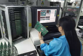
On the basis of PCB manufacturing business platform, xiangdafeng actively promotes the one-stop service mode of "PCB design → manufacturing → SMT mounting", with the goal of "creating the best overall value for the project", which eliminates the inconvenience of multi-party communication, follow-up and coordination in product design, supporting processing and production procurement process management. Through seamless connection of various business modules in the company, the cycle of customer R & D, pilot test and production is effectively shortened, the overall cost is reduced, and the one-time success rate of customer R & D projects is improved through professional technical services. To provide comprehensive R & D solutions from design, testing, debugging to verification for customers in communication, network server, photoelectric, storage and other industries.
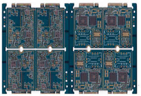
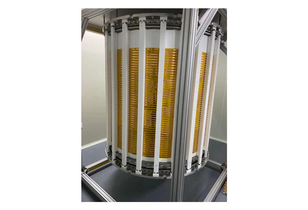
Xiangdafeng has advanced PCB production lines and test equipment, and its products are widely used in high-tech electronic fields such as communication, electronics, electric power, computer, medical equipment, instrumentation, national defense and military industry, aerospace, etc. The main products include: 4-48 layer rigid circuit board, lead-free and halogen-free environmental protection circuit board, blind buried hole circuit board, high conductivity aluminum base, thermoelectric separation copper base, iron base and metal base / core composite board, buried copper block, inlaid copper block, buried resistance and buried capacitance, ultra-thin BT board, ceramic base, Teflon (PTFE) board, high frequency mixed dielectric board, thick copper, step copper, thick gold plating, high-order HDI, flexible FPC, soft core Hard combination, super long plate, super thick plate, super small plate, etc. Materials: Rogers, Arlon, Taconic, tp-2, Megtron, neclo, Isola, f4b, Taiyao TUC, Taiguang EMC, Shengyi sy, Lianmao iteq, South Asia nouya, DuPont Kapton, etc.
Xiangdafeng takes "professionalism, integrity, quality and innovation" as its enterprise values, adheres to the road of science and technology and scientific management, adheres to the business philosophy of "based on talents and technology, providing high-quality products and services, and fully assisting customers to achieve maximum success", and has a number of high-quality management and technical talents with rich industry experience.
The company adheres to ISO9001, TS16949 quality management system, meticulously selects materials and produces attentively. All the delivered products have passed the company's strict professional performance test, with stable and reliable functions, meeting the needs of the customer market. Xiangdafeng has a special R & D team and equipment to solve all technical problems for customers. With high efficiency, high quality, high technology to provide customers with satisfactory service, so as to win the trust and support of more than 1500 customers in the global market.


PCB Production capacity
| Number of layers Layer | 2-40 layer |
|---|---|
| Sheet metal Materlal | FR4,high-TG(High TG),metal base(Metal base),high frequency(High frequency),halogen-free(Halogen free) |
| Plate thickness Board thickness | 0.15mm-8.0mm |
| Maximum size Max Panel size | 600*1200mm |
| Minimum line width / distance Min line/space | 3/3mil |
| The most small hole Min hole | Laser drilling(Laser drill) 3mil,mechanical (Mechanical drill) 0.2mm |
| Maximum aspect ratio Max asoect ratio | 12:1 |
| Copper thickness Copper thickness | 1/3 OZ to 20 OZ |
| Minimum BGA pad Min BGA PAD | 0.2mm |
| Laser blind burying HDI | 1+N+1,2+N+2, 3+N+3First order, second order, third order |
| Impedance control mpedance control | Up to +/-8% |
| Pan hole VIA in pad | yes |
| Pluging resin in hole | yes |
| PTH hole | yes |
| Back drill Back drilling | yes |
| Carbon Ink | yes |
| Blue gum Peelable solder mask ink | yes |
| Metal base Metal base | AL base,copper base,up to 4layer Aluminum base, copper base, up to 4 layers |
| Gold finger | Yes,Up to 60u" |
| Plating gold | Yes,Up to 400u" |
| Surface | OSP,HAL-leadfree,ENG,Sliver,immersion tin |
FPCProcess capability
| Category | Process capability | Category | Process capability |
|---|---|---|---|
| Type of production | Single and double sided board, multi-layer board, hollow out board, layered board, hard and soft combined board, HDI buried hole board | Number of layers | 1-14 layer FPC / 2-14 layer hard and soft composite plate and HDI buried blind hole plate |
| Maximum production size | Single and double sided board 250 * 4000mm, multilayer board 500 * 750mm | Insulation thickness | 27.5um/50um/75um/100um/125um/150um |
| Plate thickness | FPC 0.06-0.4mm、Hard and soft combination board 0.25-6.0mm | Surface treatment | Gold, Silver, Gold and tin、OSP |
| Reinforcing material | FR-4/PI/PET/SUS/PSA | Minimum line width / line spacing | 0.045mm/0.045mm |
| Copper thickness | 12um/18um/35um/70um | Minimum borehole | 0.1mm |
| Type of circuit board | Lead Time (days) | |
|---|---|---|
| PCB Type | Prototype & Pilot | Mass Production |
| 2-L | 3 | 12 |
| 4-L | 5 | 16 |
| 6-L | 5 | 18 |
| 8-L | 7 | 18 |
| 10+L | 8 | 20 |
| 4-L HDI (1+2+1) | 12 | 22 |
| 6-L HDI (1+4+1) | 14 | 24 |
| 8-L HDI (2+4+2) | 16 | 25 |
| 8-L (4+4,blind vias) | 12 | 24 |
| Aluminum PCB | 3 | 7 |
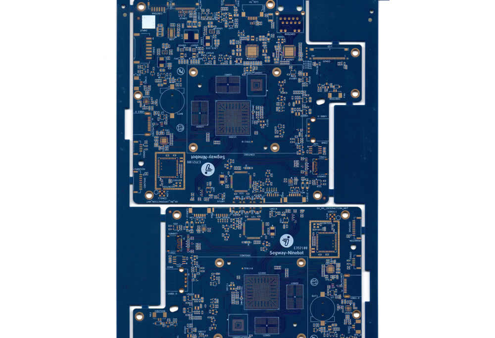
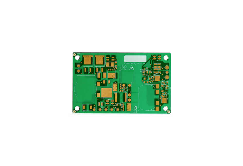
Multilayer circuit board
Number of layers: 8 layers & nbsp;
Plate thickness: 1.6 ± 0.13MM & nbsp;
Plate used: FR4 Shengyi
Minimum aperture: 0.2mm & nbsp;
Surface treatment: Gold 2U
Minimum line width / distance: 4mil / 4mil & nbsp;
Process features: high density BGA
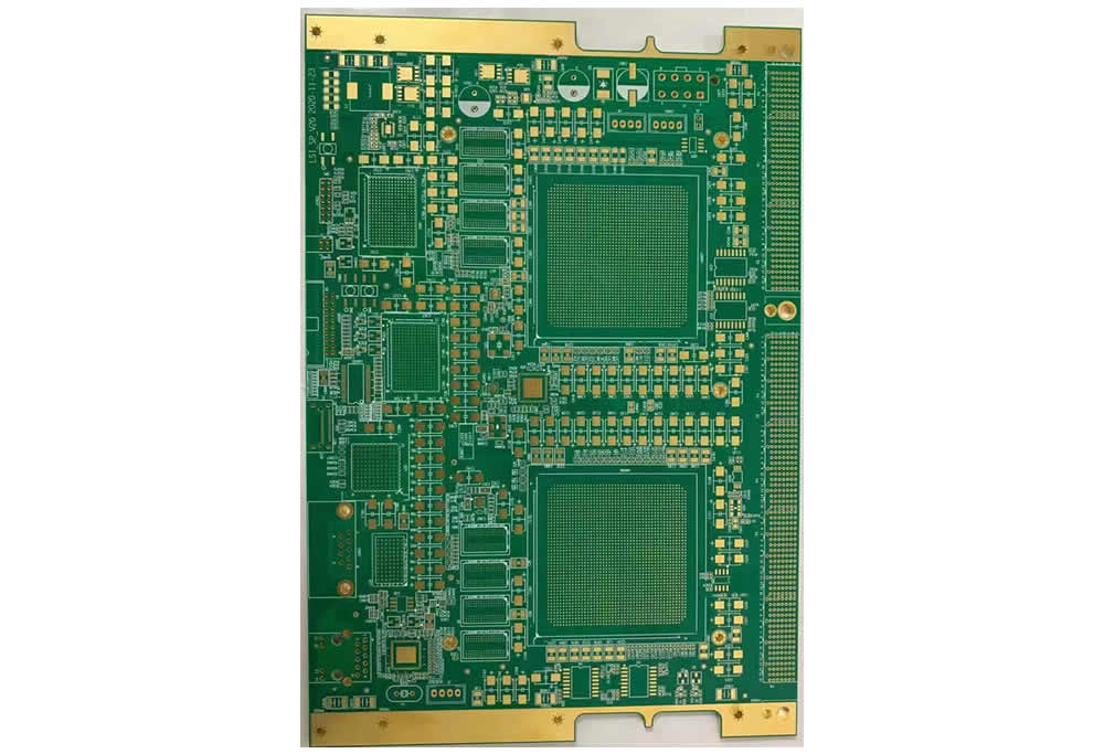
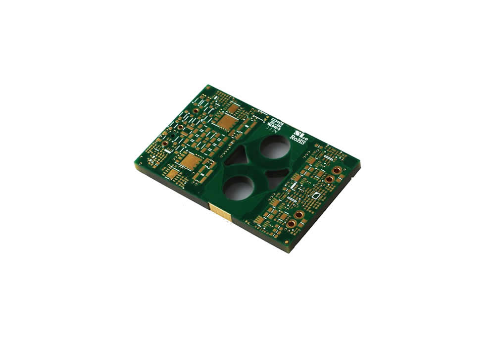
High speed back drilling circuit board
Number of floors: 12
Plate thickness: 3.0 mm
Plate used: Taiyao tu872
Surface treatment: gold deposit
Process features: first order HDI, 12 sets of back drilling, high speed plate
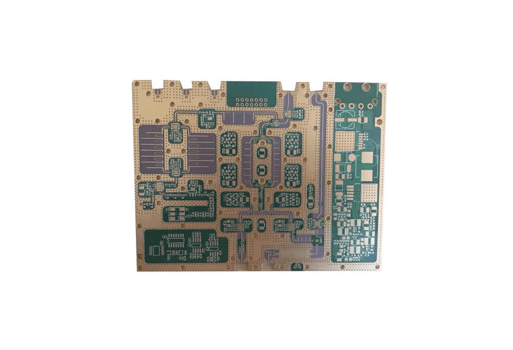
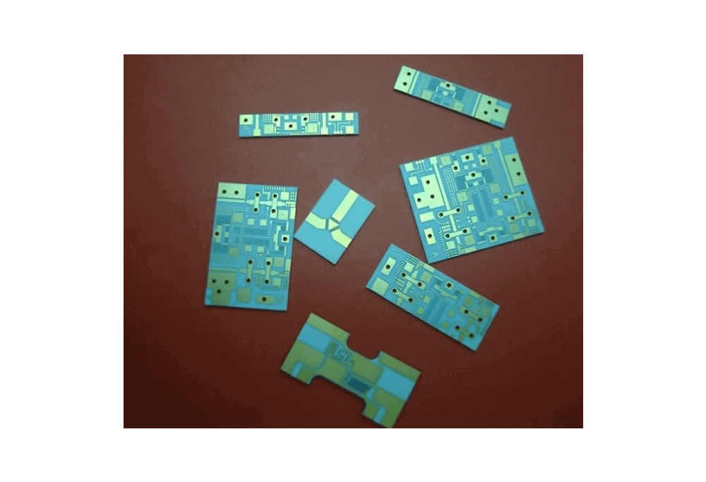
High frequency microwave circuit board
Number of layers: 2-layer plate thickness: 1.6 ± 0.13mm-nbsp;
Sheet used: polytetrafluoroethylene & nbsp;
Dielectric constant: 2.65 ± 0.05
Dielectric loss factor: 0.0037
The minimum pore size is 0.3mm & nbsp;
Surface treatment: gold deposit
Minimum line width / distance: 8mil / 8mil & nbsp;
Process characteristics: special materials and ceramic filling
Thick copper circuit board
Number of layers: 14 layers & nbsp;
Plate thickness: 3.0 + / - 0.3mm & nbsp;
Plate used: Shengyi s100-2m
Minimum aperture: 0.4mm & nbsp;
Surface treatment: gold deposit
The minimum pore size of copper: 60um & nbsp;
Inner and outer copper thickness: 160um & nbsp;
Process features: high multilayer, thick copper, metal cladding, resistance control
High aspect ratio circuit board
Number of floors: 10
Plate thickness: 5.0 mm
Plate used: FR-4
Surface treatment: gold deposit
Process features: minimum hole 0.3mm, thickness diameter ratio 1 / 16
Special ultra thick circuit board
Number of floors: 3
Plate thickness: 12mm
Plate: Isola + Rogers + FR4
Surface treatment: gold deposit
Process features: multi step drilling, super thick process
Special step circuit board
Number of floors: 3
Plate thickness: 3.2mm
Plate: Isola + Rogers + FR4
Surface treatment: deposited gold + electric thick gold 400u in
Process features: some areas protrude, some areas sag, forming steps
Ultra thin circuit board
Number of layers: 4 layers
Plate thickness: 0.4 ± 0.05mm
Plate used: FR4 Shengyi
Minimum aperture: 0.15mm
Surface treatment: Gold 2U
Minimum line width / distance: 0.1 mm / 0.1 mm
Process features: serpentine wiring, ultra thin plate thickness
HDI circuit board
Number of floors: 12
Plate thickness: 2.0 ± 0.15mm
Minimum aperture: 0.1 mm
Surface treatment: gold deposit
BGA size: 0.25mm
Minimum line width / distance: 3mil / 3mil
Blind hole structure: 1-2 layers, 2-3 layers, 3-4 layers, 9-10 layers, 10-11 layers, 11-12 layers
Process features: HDI 3 + N + 3, high density, small hole to line spacing
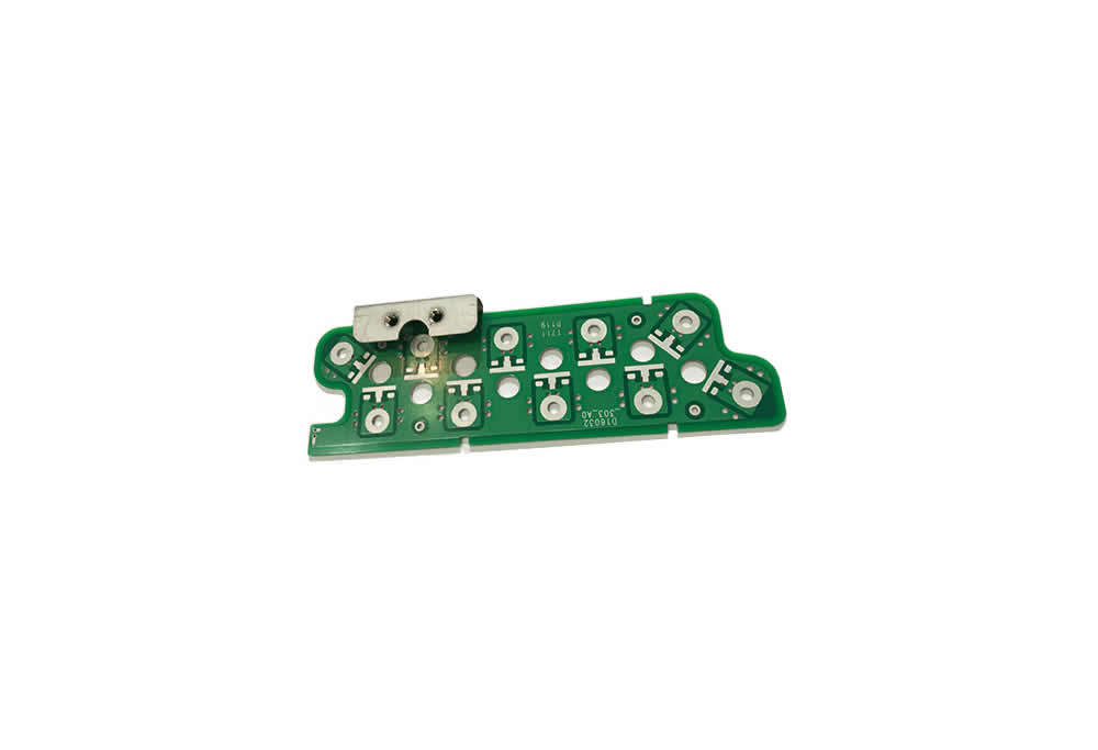
Double layer FPC
Double layer FPC
Number of floors: 2
Surface treatment: gold deposit
Process features: line width, line distance 2mil / 2mil, BGA disc hole
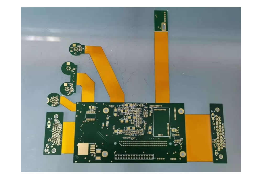
Hard and soft combination board
6-layer hard and soft composite board
Number of floors: 6
Surface treatment: gold deposit
Process features: L1, L6, FR4, tg170, L2-L5, FPC, 1.6mm drilling, L2-L3, L4-L5, 0.2mm gold finger and reinforcement
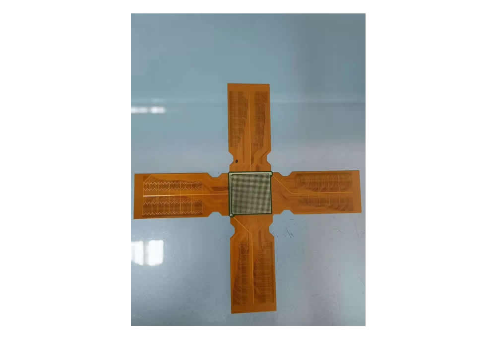
Super long FPC
Number of floors: 1
Plate thickness: 0.12mm
Surface treatment: gold deposit
Process characteristics: FPC length 3.5m
Double layer aluminum substrate
Number of layers: 2
Plate thickness: 1.6 + / - 0.1mm
Plate used: Shengyi PP + high purity aluminum
Minimum aperture: 0.3mm
Surface treatment: gold deposit
Minimum pore copper: 20um
Outer copper thickness: 35um
Process features: sandwich aluminum
Thermal conductive aluminum substrate
Number of floors: 2
Plate thickness: 1.6 + / - 0.1mm
Plate used: Shengyi + 316 stainless steel
Minimum aperture: 1.2mm
Surface treatment: Tin deposition
Minimum pore copper: 60um
Outer copper thickness: 160um
Process features: sandwich stainless steel, 3D connection
Alumina ceramic substrate
Number of floors: 1
Plate thickness: 1.0 + / - 0.1mm
Plate used: 96% alumina
Surface treatment: gold deposit
Outer copper thickness: 35um
Thermal conductivity of insulating layer: 50W
Process features: ceramic base
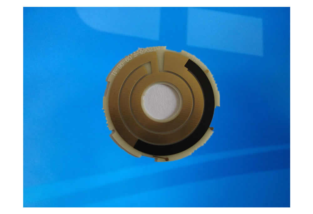
High resistance carbon film circuit board
Number of floors: 1
Plate thickness: 1.6mm
Plate used: Shengyi s1000-2m
Surface treatment: gold and carbon oil
Process features: screen printing high resistance carbon oil, accurate control of resistance
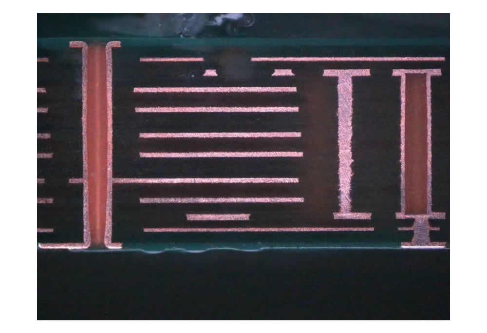
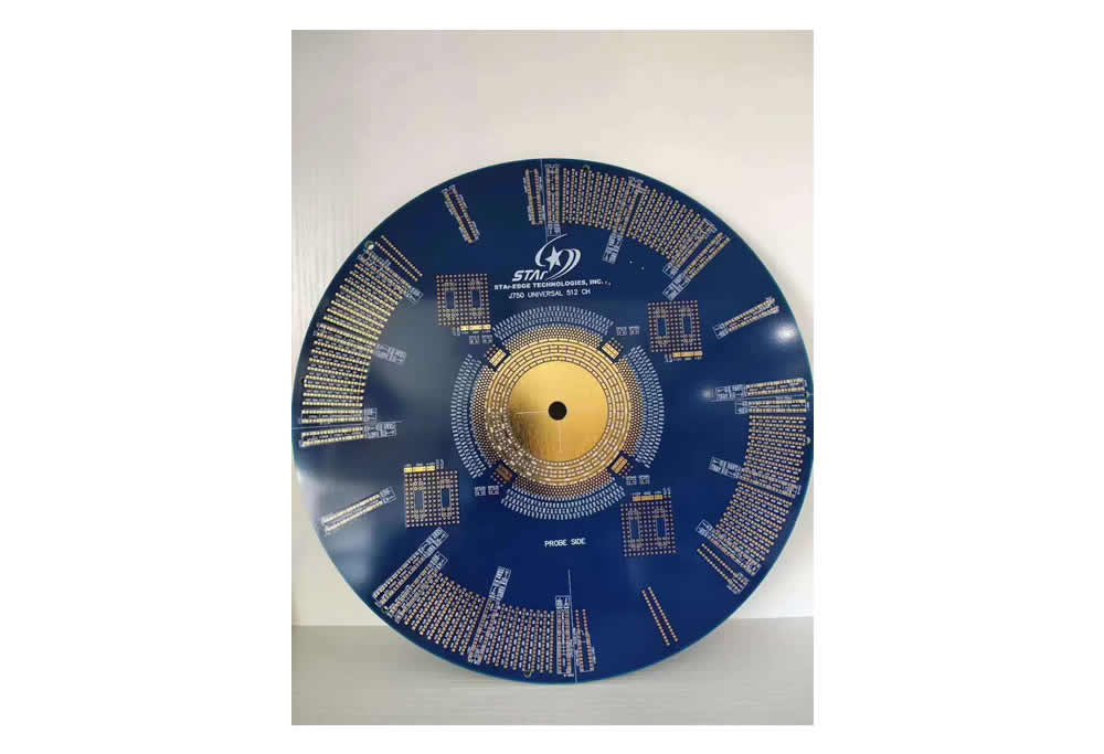
Microsection
Number of floors: 12
Plate thickness: 1.6mm
Plate used: Isola
Surface treatment: gold deposit
Process features: 2-stage HDI high-definition slice shows pore structure

Xiangdafeng Technology (Beijing) Co., Ltd Copyright No.2020041289-1
Address:712, 7th floor, building 154, brick factory Beili, Tongzhou District, Beijing
Mobile:+86 18901353186 Tel:010-82900580
Fax:010-82900580Mail:market@xdfpcba.com