


Xiangdafeng Technology (Beijing) Co., Ltd Copyright No.2020041289-1
Address:712, 7th floor, building 154, brick factory Beili, Tongzhou District, Beijing
Mobile:+86 18901353186 Tel:010-82900580
Fax:010-82900580Mail:market@xdfpcba.com
![]() Definition and classification of HDI board.xls
Definition and classification of HDI board.xls
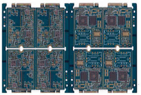
The figure below is for brief display only. Please download for details ⬆ link,~~~///(^v^)\\\~~~
Ø One order at a time:
One step at a time is also called one-step blind hole, which only connects the HDI holes of two adjacent layers directly. It refers to the HDI holes only connected by adjacent layers, such as the connection between the first layer and the second layer or / and the connection between the nth layer and the (n-1) layer. As shown in the following figure: (1 + 8 + 1 structure)

Ø Naming rules:
That is to say, 1 + X + 1: ① "1" represents the order; ② "X" represents the number of layers of inner through-hole layer; ③ there is a "1" on each side of "X" representing one order at a time;
Ø Definition:
There is only one direct connection between two adjacent layers of HDI holes, such as the connection between layer 1 and layer 2 or / and the connection between layer N and layer (n-1). (n represents the number of layers of the board, the same below), as shown in the figure below:


Three key processes in HDI PCB......
Why plug holes should be made ......
Analysis of the main causes of......
PCB design company analyzes th......
PCB via design specification...
The type selection of componen......
Common PCB high frequency and ......
Factors affecting PCB cost...
SMT customer incoming material......
Definition and classification ......
Consultation hotline
010-82900580
Xiangdafeng Technology (Beijing) Co., Ltd Copyright No.2020041289-1
Address:712, 7th floor, building 154, brick factory Beili, Tongzhou District, Beijing
Mobile:+86 18901353186 Tel:010-82900580
Fax:010-82900580Mail:market@xdfpcba.com