


Xiangdafeng Technology (Beijing) Co., Ltd Copyright No.2020041289-1
Address:712, 7th floor, building 154, brick factory Beili, Tongzhou District, Beijing
Mobile:+86 18901353186 Tel:010-82900580
Fax:010-82900580Mail:market@xdfpcba.com
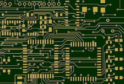
HDIPCB is the most precise PCB, and its manufacturing process is also the most complex. The key steps are the formation of high precision printed circuit, the processing of micro via and the electroplating of surface and hole. Next, let's take a look at these core steps in HDI PCB plate making.
1、 Ultra fine circuit processing
With the development of science and technology, some high-tech equipment is becoming more and more miniaturized and precise, which requires higher and higher HDI board. The line width / line distance of HDI circuit board of some equipment has developed from 0.13 mm (5 mil) to 0.075 mm (3 mil), and has become the mainstream standard. As a leading enterprise in HDI Allegro industry, xiangdafeng technology's related production process has reached 38 μ m (1.5 mil), which is close to the limit of the industry.
The increasing requirements of line width / line distance bring the most direct challenge to the graphics imaging in the process of PCB manufacturing. So how are the copper wires on these precision boards processed?
At present, the formation process of fine circuit includes laser imaging (pattern transfer) and pattern etching. Laser direct imaging (LDI) technology is to get fine circuit graphics by laser scanning directly on the surface of copper clad laminate coated with photoresist. Laser imaging technology greatly simplifies the process flow and has become the mainstream technology in HDI PCB plate making.
Now the application of semi addition method (SAP) and improved semi addition method (masap) is more and more, that is, pattern etching method. This technology can also achieve 5um line width of conductive lines.
2、 Micropore processing
The important feature of HDI circuit board is that it has micro through holes (aperture ≤ 0.10 mm), which belong to buried blind hole structure. At present, the blind holes on HDI board are mainly processed by laser, but there are also CNC drilling.
Compared with laser drilling, mechanism drilling also has its own advantages. When the through-hole of epoxy glass cloth dielectric layer is processed by laser, the quality of the through-hole will be slightly poor due to the difference of ablation rate between the glass fiber and the surrounding resin, and the reliability of the through-hole will be affected by the residual glass fiber on the hole wall. Therefore, the superiority of mechanical drilling at this time is reflected. In order to improve the reliability and drilling efficiency of PCB, laser drilling and mechanical drilling technology are steadily improved.
3、 Electroplating and surface finishing

In PCB manufacturing, how to improve the plating uniformity and deep hole plating ability, and improve the reliability of the board. This depends on the continuous improvement of electroplating process, from the proportion of electroplating solution, equipment deployment, operation process and other aspects.
High frequency sound wave can accelerate the etching ability; permanganate solution can enhance the decontamination ability of the workpiece; high frequency sound wave will stir and add a certain proportion of potassium permanganate electroplating solution in the electroplating bath. This helps the bath flow into the hole evenly. So as to improve the deposition ability and uniformity of copper plating.
At present, copper plating and filling of blind holes are mature, and through holes with different diameters can be filled with copper. The two-step copper plating filling method is suitable for through holes with different pore sizes and high thickness to diameter ratio. It has strong copper filling ability and can reduce the thickness of the surface copper layer as much as possible.
There are many options for the final surface finishing of PCB. Electroless nickel / gold (ENIG) and electroless nickel / palladium / gold (ENEPIG) are widely used in high-end PCB.
Both ENIG and ENEPIG have the same gold dipping process. It is very important to select the appropriate gold dipping process for reliable installation and welding or wire bonding. There are three types of gold leaching processes: standard displacement gold leaching, high efficiency gold leaching with limited nickel dissolution, and reduction reaction gold leaching with mixed mild reducing agents. Among them, the effect of reduction leaching is better.
For the problem that the nickel layer in ENIG and ENEPIG coatings is not conducive to high frequency signal transmission and the formation of fine lines, electroless palladium / catalytic gold plating (EPAG) can be used instead of ENEPIG to remove nickel, so as to reduce the metal thickness.
Three key processes in HDI PCB......
Why plug holes should be made ......
Analysis of the main causes of......
PCB design company analyzes th......
PCB via design specification...
The type selection of componen......
Common PCB high frequency and ......
Factors affecting PCB cost...
SMT customer incoming material......
Definition and classification ......
Consultation hotline
010-82900580
Xiangdafeng Technology (Beijing) Co., Ltd Copyright No.2020041289-1
Address:712, 7th floor, building 154, brick factory Beili, Tongzhou District, Beijing
Mobile:+86 18901353186 Tel:010-82900580
Fax:010-82900580Mail:market@xdfpcba.com