


Xiangdafeng Technology (Beijing) Co., Ltd Copyright No.2020041289-1
Address:712, 7th floor, building 154, brick factory Beili, Tongzhou District, Beijing
Mobile:+86 18901353186 Tel:010-82900580
Fax:010-82900580Mail:market@xdfpcba.com
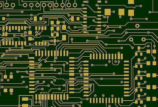
1、 PCB design impedance matching
PCB design impedance matching refers to a suitable matching between signal source or transmission line and load. According to the access mode, PCB design impedance matching has two ways: serial and parallel; according to the signal source frequency, PCB design impedance matching can be divided into low frequency and high frequency.
High frequency signal usually uses serial PCB to design impedance matching
The resistance value of the serial resistor is 20 ~ 75 Ω, which is directly proportional to the signal frequency and inversely proportional to the PCB wiring width. In the embedded system, when the frequency is more than 20m and the length of PCB is more than 5cm, the serial matching resistance should be added, such as the clock signal, data and address bus signal in the system. There are two functions of serial matching resistor
Reduce high frequency noise and edge overshoot. If the edge of a signal is very steep, it contains a large number of high-frequency components, which will radiate interference, in addition, it is easy to produce overshoot. The series resistance, distributed capacitance of signal line and load input capacitance form an RC circuit, which will reduce the steepness of signal edge.
2. Reduce high frequency reflection and self-excited oscillation. When the frequency of the signal is very high, the wavelength of the signal is very short. When the wavelength is short enough to match the length of the transmission line, the reflection signal superimposed on the original signal will change the shape of the original signal. If the characteristic impedance of the transmission line is not equal to the load impedance (that is, it does not match), reflection will occur at the load end, resulting in self-excited oscillation. The low-frequency signal of PCB can be directly connected, generally without adding serial matching resistance.

Parallel PCB design impedance matching is also called "terminal PCB design impedance matching"
Generally used in the input / output interface, it mainly refers to the impedance matching with the PCB design of the transmission cable. For example, the input matching resistance of LVDS and RS422 / 485 using type 5 twisted pair is 100 ~ 120 Ω; the matching resistance of video signal using coaxial cable is 75 Ω or 50 Ω, and that using flat cable is 300 Ω. The resistance value of parallel matching resistance is related to the medium of transmission cable and has nothing to do with the length. Its main function is to prevent signal reflection and reduce self-excited oscillation.
It is worth mentioning that the impedance matching of PCB design can improve the EMI performance of the system. In addition, in order to solve the impedance matching of PCB design, in addition to using series / parallel resistance, transformer can also be used for impedance transformation, such as Ethernet interface, can bus and so on.
2、 Zero ohm resistance
1. The simplest way is to make jumper. If a certain section of line is not used, the resistance can be directly not welded (without affecting the appearance).
2. When the parameters of the matching circuit are uncertain, it is replaced by zero ohm. In actual debugging, the parameters are determined, and then the components with specific values are replaced.
3. When you want to measure the working current of a certain part of the circuit, you can remove the zero ohm resistance and connect the ammeter, which is convenient to measure the current.
4. In the PCB design and wiring, if it can not be laid, you can also add a zero ohm resistor to play a bridging role.
5. In the high frequency signal network, it acts as an inductor or capacitor (plays the role of PCB design impedance matching, and zero ohm resistance also has impedance). When used as an inductor, it is mainly to solve the EMC problem.
6. Single point grounding, such as single point grounding of analog ground and digital ground.
7. Configuration circuit can replace jumper and dial switch. Sometimes the user will tamper with the settings, which is easy to cause misunderstanding. In order to reduce the maintenance cost, zero ohm resistance is used instead of jumper to weld on the board.
8. System commissioning, for example, the system is divided into several modules, the power supply between the modules is separated from the ground by zero ohm resistance, when the power supply or ground short circuit is found in the commissioning stage, the search range can be reduced by removing the zero ohm resistance.
The above functions can also be replaced by magnetic beads. Although the function of zero ohm resistance is similar to that of magnetic bead, there are essential differences between them. The former has impedance characteristics, while the latter has inductive characteristics. Magnetic beads are generally used in power and ground network, and have filtering function.

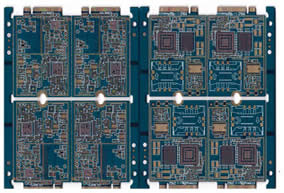
PCB design capability
Maximum signal design rate: 10Gbps CML differential signal;
Maximum number of PCB design layers: 40 layers;
Minimum line width: 2.4 mil;
Minimum line spacing: 2.4mil;
Minimum BGA pin spacing: 0.4mm;
Minimum mechanical hole diameter: 6mil;
The minimum diameter of laser drilling is 4mil;
Maximum number of pins:; 63000+
Maximum number of components: 3600;
Maximum number of BGAs: 48 +.
Three key processes in HDI PCB......
Why plug holes should be made ......
Analysis of the main causes of......
PCB design company analyzes th......
PCB via design specification...
The type selection of componen......
Common PCB high frequency and ......
Factors affecting PCB cost...
SMT customer incoming material......
Definition and classification ......
Consultation hotline
010-82900580
Xiangdafeng Technology (Beijing) Co., Ltd Copyright No.2020041289-1
Address:712, 7th floor, building 154, brick factory Beili, Tongzhou District, Beijing
Mobile:+86 18901353186 Tel:010-82900580
Fax:010-82900580Mail:market@xdfpcba.com