


Xiangdafeng Technology (Beijing) Co., Ltd Copyright No.2020041289-1
Address:712, 7th floor, building 154, brick factory Beili, Tongzhou District, Beijing
Mobile:+86 18901353186 Tel:010-82900580
Fax:010-82900580Mail:market@xdfpcba.com
Why plug holes should be made in PCB manufacturing? Via hole is also called via hole. In order to meet the requirements of customers, the via hole of circuit board must be plugged. After a lot of practice, the traditional process of plugging hole of aluminum sheet is changed, and the resistance welding and plugging hole of circuit board surface are completed with white net. The production is stable and the quality is reliable.

Via hole plays an important role in the interconnection of circuits. With the development of electronic industry, it also promotes the development of PCB, and puts forward higher requirements for PCB manufacturing process and SMT processing technology. Via hole plug technology came into being, and the following requirements should be met:
1. The copper in the through hole is enough, and the resistance welding can be plugged or not;
2. There must be tin and lead in the through hole, with a certain thickness requirement (4 microns), no solder resist ink into the hole, causing tin beads in the hole;
3. The through hole must have solder resist ink plug hole, not transparent, no tin ring, tin bead and leveling requirements.
With the development of electronic products in the direction of "light, thin, short and small", PCB is also developing towards high density and high difficulty. Therefore, a large number of SMT and BGA PCBs appear. Customers require plug holes when mounting components, which mainly have five functions
1. To prevent short circuit caused by tin penetrating through the element surface during PCB over wave soldering; especially when we put the through hole on the BGA pad, we must first make the plug hole and then gold plating to facilitate BGA soldering.
2. Avoid flux remaining in the through hole;
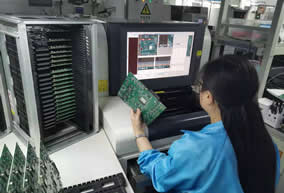
3. After SMT processing and component assembly in electronics factory, PCB should be vacuumed to form negative pressure on testing machine
4. Prevent the surface solder paste from flowing into the hole to cause false soldering and affect the mounting;
5. Prevent solder bead from popping out during over wave soldering, resulting in short circuit.

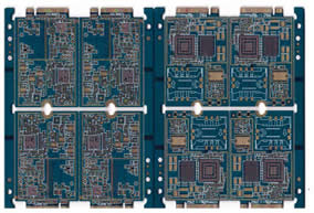
Xiangdafeng's advantages in PCB manufacturing
1. Energy production 2-14 layers, 14-22 layers can be proofed.
2. Minimum line width / spacing: 3mil / 3mil BGA spacing: 0.20mm
3. Minimum aperture of finished product: 0.1 mm, size: 610 mmx1200 mm
4. Ink: Tamura, Taiyo, fudoken, Japan;
5. FR4: Shengyi, Jiantao, Haigang, Hongren, Guoji, Hezheng, South Asia
(Shengyi s1130 / S1141 / s1170), tg130 ℃ / tg170 ℃, tg180 ℃ and other high Tg plates)
6. High frequency board: Rogers, Taconic, arllon;
7. Surface technology: tin spraying, lead-free tin spraying, gold precipitation, whole plate gold plating, plug gold plating, whole plate thick gold, chemical tin precipitation (silver), anti-oxidation (OSP) blue glue, carbon oil.
Three key processes in HDI PCB......
Why plug holes should be made ......
Analysis of the main causes of......
PCB design company analyzes th......
PCB via design specification...
The type selection of componen......
Common PCB high frequency and ......
Factors affecting PCB cost...
SMT customer incoming material......
Definition and classification ......
Consultation hotline
010-82900580
Xiangdafeng Technology (Beijing) Co., Ltd Copyright No.2020041289-1
Address:712, 7th floor, building 154, brick factory Beili, Tongzhou District, Beijing
Mobile:+86 18901353186 Tel:010-82900580
Fax:010-82900580Mail:market@xdfpcba.com